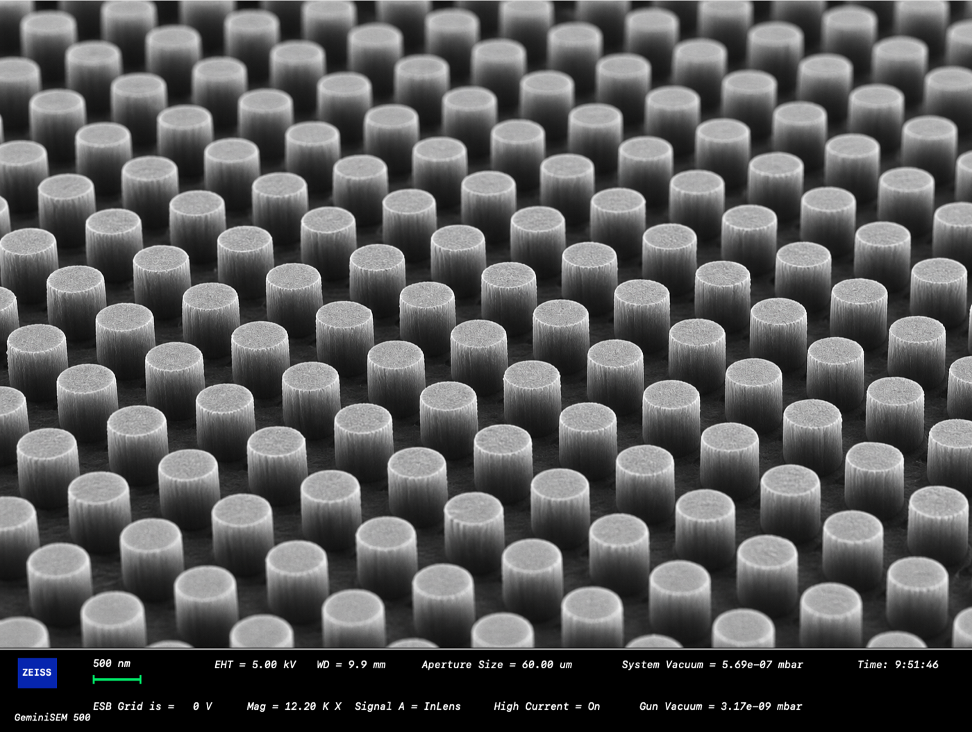
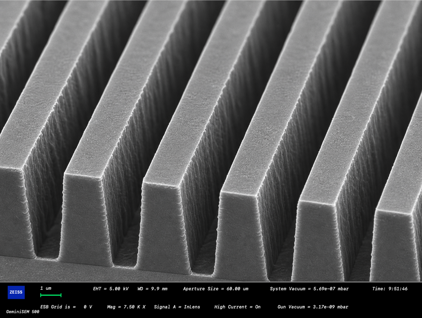
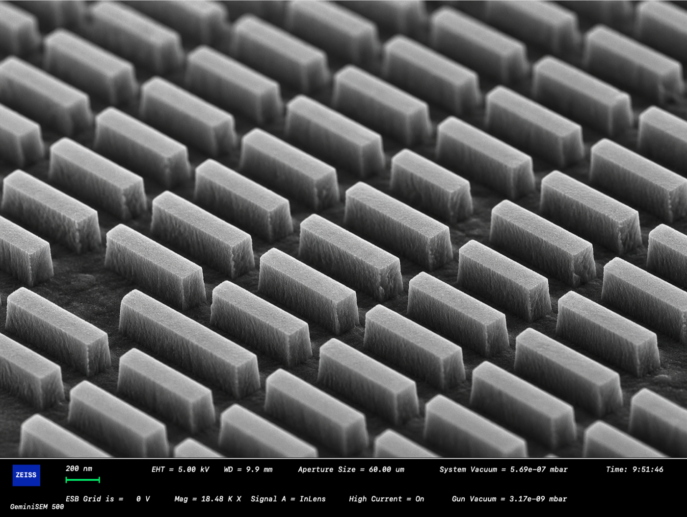
电子束/DUV/激光直写EBL / DUV / Laser Writing
支持纳米级图形、母版、超表面与光栅结构,适配科研样品、小批量验证和晶圆级图形化。For nanoscale patterns, masters, metasurfaces and gratings, covering research samples, pilot runs and wafer-level patterning.
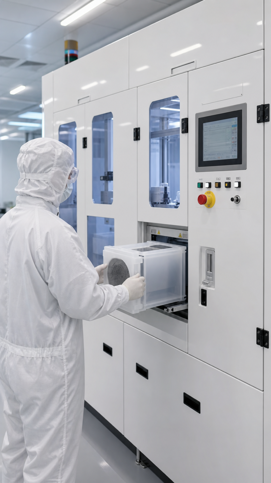
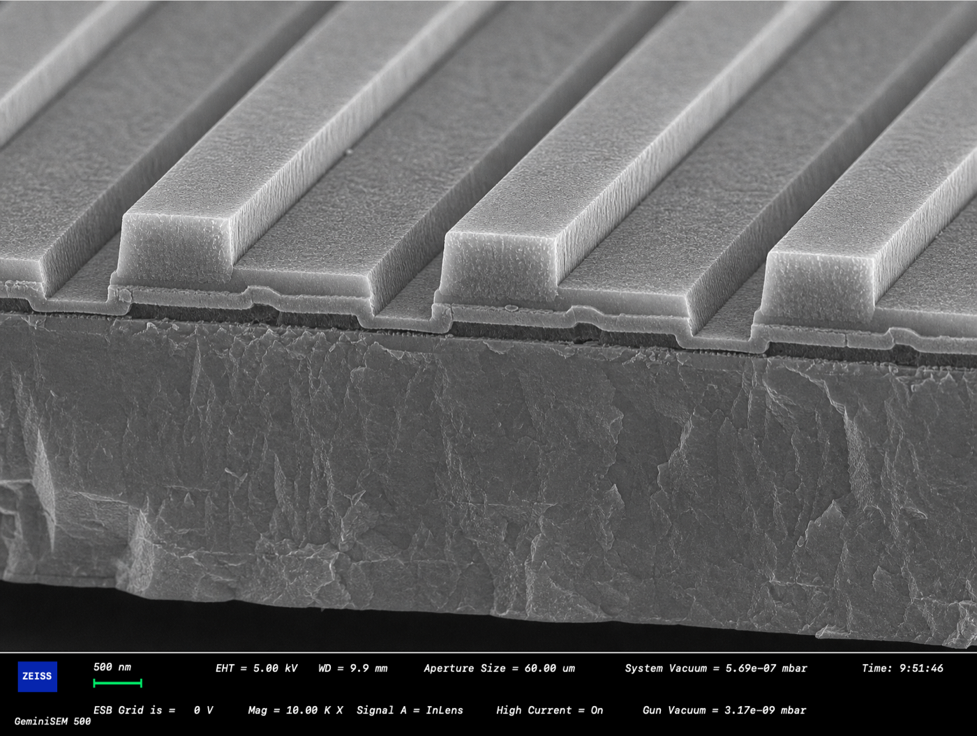
半导体微纳制造服务平台 Semiconductor Micro/Nano Fabrication
面向科研机构、光电企业和半导体团队,提供从版图评审、电子束/DUV/激光直写、刻蚀转移、薄膜与清洗,到 SEM/电学/RF 测试的工艺协同服务。 Integrated process support for research labs, photonic companies and semiconductor teams, from layout review, EBL/DUV/laser lithography and etch transfer to thin films, cleaning, SEM, electrical and RF testing.
关于我们About Us
微纳加工聚焦半导体与光电子芯片工艺服务,面向超表面、超透镜、光栅、波导、MEMS、生物芯片、传感器和高精度掩膜板等方向,提供“小批量、多工艺、强验证”的加工支持。 MicroNano Fabrication focuses on semiconductor and optoelectronic chip process services for metasurfaces, metalenses, gratings, waveguides, MEMS, biochips, sensors and high-precision photomasks, with flexible small-batch manufacturing and verification support.
网站内容参考了本地宣传册、英文版资料、去标识商品素材与 SEM/洁净室视觉素材,定位更偏企业官网:专业、克制、面向项目转化。 The site positioning is built from internal brochures, English presentation material, cleaned product visuals, SEM imagery and cleanroom assets: professional, restrained and project-conversion oriented.
产品服务Services
按项目目标匹配工艺路线,减少客户在设备、材料、版图和检测之间反复试错。 Process routes are matched to project goals, reducing iteration across equipment, materials, layouts and metrology.
支持纳米级图形、母版、超表面与光栅结构,适配科研样品、小批量验证和晶圆级图形化。For nanoscale patterns, masters, metasurfaces and gratings, covering research samples, pilot runs and wafer-level patterning.
覆盖 RIE、DRIE、IBE、湿法刻蚀、释放结构与高深宽比结构,服务硅、石英、氮化硅、TiO2 等材料体系。RIE, DRIE, IBE, wet etch, release processes and high-aspect-ratio structures for silicon, quartz, SiN, TiO2 and more.
支持金、铬、铜、铂、钨等金属薄膜与功能薄膜工艺,适用于电极、传感器、MEMS 和光电子器件。Metal and functional films including Au, Cr, Cu, Pt and W for electrodes, sensors, MEMS and optoelectronic devices.
面向电子束曝光后的显影、去胶、RCA/湿法清洗、载具转运与样品入盒,保障样品洁净和交付一致性。Development, resist removal, RCA/wet cleaning, carrier transfer and sample packaging after lithography.
可结合 SEM 表征、IV/CV、RF、噪声分析与探针台测试,为工艺窗口、良率和器件性能提供数据依据。SEM, IV/CV, RF, noise analysis and probe-station testing support process windows, yield review and device performance checks.
可延展至晶圆、PCB、芯粒、PD、光波导片等外观缺陷检测与自动化测试设备方案。Extensible to AOI and automation solutions for wafers, PCB substrates, dies, PD chips and optical waveguide sheets.
能力矩阵Capability Matrix
案例Cases
从光学超构表面到 MEMS 深硅结构,案例展示以工艺能力和可验证结果为核心。 From optical metasurfaces to MEMS deep silicon structures, cases focus on process capability and verifiable outputs.
支持 TiO2、SiN、Si、Ge 等材料体系,围绕相位调控、偏振控制、成像和传感应用进行结构制备。Supports TiO2, SiN, Si and Ge systems for phase control, polarization, imaging and sensing applications.
确认材料、版图、目标 CD、深度、晶圆尺寸、交付数量和测试要求。Confirm material, layout, target CD, depth, wafer size, quantity and test goals.
选择曝光、显影、刻蚀、镀膜、Lift-off、清洗和检测组合。Select lithography, development, etch, coating, lift-off, cleaning and inspection steps.
按工艺窗口推进样品,关键步骤保留过程记录和异常反馈。Run samples through the process window with records and exception feedback.
输出 SEM/测试数据、样品入盒、交付说明和下一轮优化建议。Deliver SEM/test data, packaged samples, notes and next-round optimization suggestions.
新闻News
围绕 TiO2、SiN、SOI、Ge 等材料,梳理不同波段的工艺节点和 SEM 验证策略。Process nodes and SEM verification strategy for TiO2, SiN, SOI and Ge across UV, VIS, NIR and MIR bands.
以深硅槽、纳米柱、光栅母版为例,评估深宽比、侧壁粗糙度、残胶和清洗对成品的影响。A review of aspect ratio, sidewall roughness, residue and cleaning for trenches, nano-pillars and grating masters.
建议客户在项目初期同步准备版图文件、材料参数、目标尺寸、公差、测试方式和交付节奏。Recommended early-stage inputs: layout files, material parameters, target dimensions, tolerance, tests and delivery rhythm.
联系我们Contact
建议包含:材料体系、晶圆/样品尺寸、目标线宽或周期、刻蚀深度、数量、是否需要 SEM/电学/RF 测试、期望交付时间。 Recommended inputs: material system, wafer/sample size, target CD or period, etch depth, quantity, SEM/electrical/RF test needs and expected delivery date.